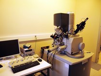
FEI Nova 600 Nanolab Dual-Beam FIB
SEM (Scanning Electron Microscope) can be used for inspection of samples with resolution down to nanometer scale. The FIB (Focused Ion Beam) column can be used for making cross-sections in virtually any material and gives the option to look "into" the material. FIB also allows to directly pattern materials with nanometer resolution. Options include electron backscatter diffraction (EBSD, for evaluation of microstructure of material), several etch gas injectors, Auto-slice&View and nanomanipulators for TEM-slice preparation.
Specifications
Our Dual-Beam FIB is fully equipped and consists of:
- SEM column: a Sirion Field-Emission Gun electron source (FEG-SEM (30kEV, sub 2nm resolution)
- ION column: Magnum system with a Gallium Liquid metal ion source (LMIS) (30kEV, fabrication of sub-100nm structures)
- HKL-EBSD system
- 3 Gas Injectors Systems including Pt deposition, Delineation etch (TFA) for SiO2 and Selective Carbon Mill (H2O) for polymers
- Basic detectors: ETD, TLD
- Extra: CDEM-detector, low-kV Solid-state on-axis BSE-detector, Solid-state STEM-detector
- Possibility for handling 200mm wafers
- Microprobe and possibility for automatic TEM-sample preparation (Auto-Fib, Auto-Tem and Auto-slice&View)
- Located in clean-room environment.
Applications
- Cross-section analysis
- Patterning
- Crystallographic orientation imaging
- TEM-slice preparation
- Chip Repair (failure analysis or device modification)
