Synchrotron experiments
In situ characterization of film growth
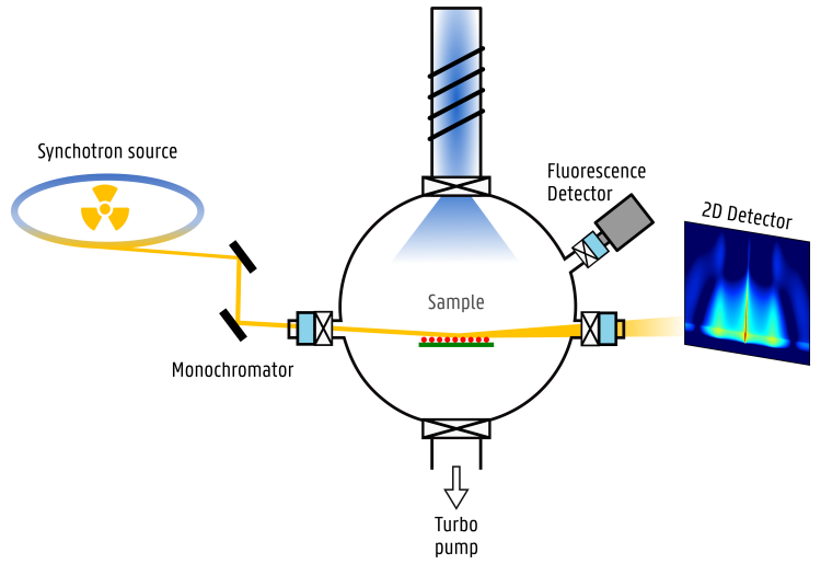
The CoCooN research group has pioneered the use of synchrotron-based X-ray techniques for in situ characterization during ALD. By shining X-rays into an ALD reactor, a variety of X-ray based techniques that have been developed to study surfaces and films can be used to study ALD growth. For example, we demonstrated the unique suitability of in situ x-ray fluorescence (XRF) and grazing incidence small angle x-ray scattering (GISAXS) for monitoring, respectively, the amount of deposited material and the evolution in surface roughness during ALD. A dedicated ALD system was built for in situ X-ray studies at synchrotron beamlines. This system allows for thermal and plasma-enhanced ALD in combination with several X-ray based characterization techniques, such as X-ray reflectivity (XRR), X-ray absorption spectroscopy (XAS), XRF and GISAXS.
Publications:
Devloo-Casier, Kilian, et al. “In Situ Synchrotron Based X-ray Techniques as Monitoring Tools for Atomic Layer Deposition.” JOURNAL OF VACUUM SCIENCE & TECHNOLOGY A 32, 1 (2014). DOI: 10.1116/1.4851716
Filez, Matthias, et al. “Formation and Functioning of Bimetallic Nanocatalysts : The Power of X-Ray Probes.” ANGEWANDTE CHEMIE-INTERNATIONAL EDITION, vol. 58, no. 38, 2019, pp. 13220–30. DOI: 10.1002/anie.201902859
Texture of thin films
Texture, or the statistical distribution of grain orientation, is an important characteristic of the microstructure of poly-crystalline films. Texture is known to influence e.g. the mechanical, magnetic and thermoelectrical properties of thin films. Therefore, controlling texture is important for many applications.
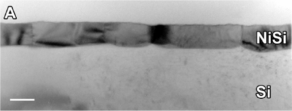
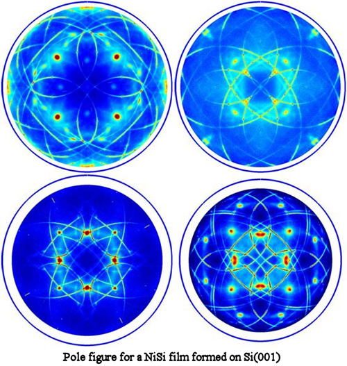
In present day Si-based micro-electronics, metal-Si compounds are used to contact the active regions of the transistor. These silicide layers are usually formed by a solid-state reaction between a deposited metal film and the Si substrate. The continued decrease in line width makes it increasingly important to characterize and control the microstructure of the silicide film. Indeed, in some cases silicide lines are in fact bamboo structures of a single row of grains. The orientation or texture of these grains will determine their interface structure and energy, and therefore influence important properties such as work function, barrier height, contact resistance, agglomeration resistance and phase formation sequence. Although a lot of effort was undertaken to optimize the epitaxial growth of certain silicides that have a good lattice match to Si, little is known regarding the texture of 'standard' silicide films (i.e. for silicide phases where no lattice match is expected). Pioneering work on texture analysis for silicide films was performed by Bulle-Lieuwma et al. for CoSi2 [1] and by Ozcan et al. for TiSi2 [2]. In past years, we have made a detailed study of the texture of various silicide phases. For NiSi layers, we observed complex patterns on the pole figures which could not be explained on the basis of the existing classification of texture in thin films. Further research showed that several silicide phases (NiSi, CoSi2 , alpha-FeSi2) exhibit a new type of texture, which we called 'axiotaxy'. Axiotaxy (1D periodic interface) can be considered as an intermediate case between epitaxy (2D periodicity) and a random interface (no periodicity).
More information on thin film texture can be found in our review paper. Find out about GUSTAV, an in-house developed software package for the analysis and visualization of thin film texture.
Literature and publications:
Bulle-Lieuwma, C.W.T., et al. “Observation and analysis of epitaxial growth of CoSi2 on (100) Si.” JOURNAL OF APPLIED PHYSICS 71, 2211 (1992). DOI: 10.1063/1.351119
Özcan, A.S., et al. “Texture of TiSi2 thin films on Si (001).” JOURNAL OF APPLIED PHYSICS 92, 5011 (2002). DOI: 10.1063/1.1509849
De Schutter, Bob et al. “Texture in Thin Film Silicides and Germanides : a Review.” APPLIED PHYSICS REVIEWS 3.3 (2016). DOI: 10.1063/1.4960122


