Research at LumiLab
The research of LumiLab is mainly focused on inorganic luminescent materials (also known as phosphors). We study the relation between the structural, electronic and optical characteristics of these materials. Read more about our topics below or browse through our publications.
- White-LED phosphors
- Infrared phosphors
- Persistent luminescence
- Mechanoluminescence
- Switchable materials
- Photocatalytically active materials
- Electronic structure of luminescent materials
- Microscopic cathodoluminescence spectroscopy
Over the years LumiLab has acquired an extensive set of analytical techniques for studying phosphors. This includes e.g. high performance UV-Vis-NIR spectrophotometry, photoluminescence excitation, emission and decay spectroscopy, electron microscopy, and thermoluminescence spectroscopy. A complete overview of our equipment can be found under facilities .
In addition to several research collaborations, the LumiLab team at Ghent University regularly receives visitors from all over the world. LumiLab remains open to all kinds of new formal or informal collaborations in the future.
White-LED phosphors
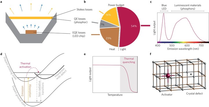
Phosphors are key components in solid state lighting, where they convert partly or entirely the emission of the pumping LED to longer wavelengths, in order to achieve the desired spectral distribution. Efficient and temperature stable phosphors with specific excitation and emission spectra are developed, in order to realize LEDs with high color gamut or high color rendering, in the case of display backlighting or general lighting, respectively. At LumiLab we have mainly been working on narrowband europium doped sulfide (SrGa2S4:Eu2+, (Ca,Sr)S:Eu2+), (oxy)nitride and red Mn4+ doped fluoride K2SiF6 phosphors. For this research we focused on photoluminescence properties, quantum efficiency, non-radiative decay paths, energy transfer due to doping inhomogeneities… We also investigate the influence of temperature and the material stability. The impact of protective coatings prepared by atomic layer deposition (ALD) has been studied in collaboration with the CoCooN group.
Infrared emitting phosphors
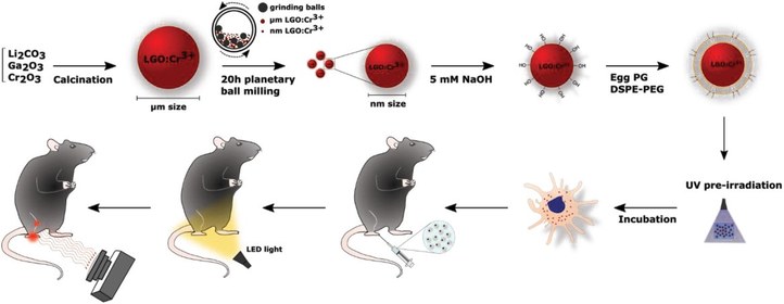
Most phosphor materials emit in the visible range. However, there is also a strong interest in near-infrared emitting nanoparticles. Skin, biological tissues and even bone are partially transparent in the near infrared, which enables tracking the position of IR-emitting particles from outside the body. Such particles could replace and supplement radioactive tracers in a wide range of applications, and be used during surgery, in cancer immunotherapy and for tracking drug delivery. Within LumiLab, nanoscale phosphors with suitable excitation and emission properties are investigated. Toxicity testing and finally in vivo testing are conducted in collaboration with departments of pharmacy and medicine.
Persistent luminescence
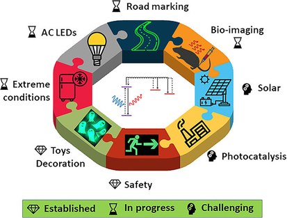
Persistent phosphors are luminescent materials that are functionalized by purposely introducing specific intrinsic (e.g. vacancies or interstitials) and extrinsic defects (e.g. by codoping the phosphor with other metal ions such as the trivalent lanthanides). Thanks to the presence of these trapping defects the luminescence lifetime can be extended from a few micro- or milliseconds up to minutes, hours or even days depending on the (thermal) stability of the trapped charge. This persistent luminescence is widely exploited in glow-in-the-dark features or non-electrical safety signage but persistent phosphors also hold great potential to be used for photocatalysis, in vivo bioimaging, photodynamic therapy or stress sensing applications. The focus of persistent phosphor research in LumiLab lies in the use of thermoluminescence and optically stimulated luminescence spectroscopy to study and identify the chemical nature of the relevant trapping defects and to uncover the microscopic mechanism behind this fascinating phenomenon.
Mechanoluminescence
Mechanoluminescence (ML) is the light emission due to mechanical stimulus of persistent phosphors. ML phosphors often possess crystal defects that can store charges upon optical excitation (i.e. charging). These trapped electrons can escape traps (i.e. detrapping) with the help of thermal energy or mechanical stress. The complexity of mechanical detrapping involves the subtle interplay among the elastic properties of the ML phosphor, the piezoelectricity of the phosphor, and the electronic structure of the traps. The research of LumiLab aims at understanding how and why stress releases the trapped electrons. This leads to a quantitative relationship between ML intensity and the given loading profiles, paving the way for accurate ML sensors.
Switchable materials
Photochromic materials
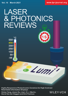
Photochromic materials can switch between two states with different absorption spectra, and thus different color appearance, under the influence of light irradiation. Because of the optical difference between the two states, photochromic materials exhibit great potential for light-driven devices such as optical data storage, smart windows and security printing. However, there are still some characteristics that need improvement for use in practical applications, such as response rate, fatigue resistance and chemical stability. Our research mainly focuses on identifying the relevant parameters during the photochromic transition, designing multicolor photochromic materials, using the photochromic behavior to modulate reflectivity and luminescence intensity, and eventually designing some prototype devices e.g. a hand-rewritable display.
Samarium Monosulfide
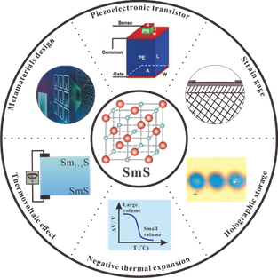
Samarium monosulfide (SmS) is a typical switchable material, which undergoes a pressure-induced semiconductor-to-metal transition at a critical pressure Pc≈6.5 kbar and room temperature. The dramatic changes of its optical, electrical and magnetic properties during this phase transition make SmS a very promising material for use in strain gauges, piezoelectronic transistors, and high-density optical storage. Most of these applications require high-quality SmS thin films, while the corresponding study is still at a primary stage. LumiLab applies electron beam evaporation for the fabrication of SmS thin films after which quality is assessed by a thorough investigation of their piezoresistive response and photoconductive properties.
Photocatalytically active materials
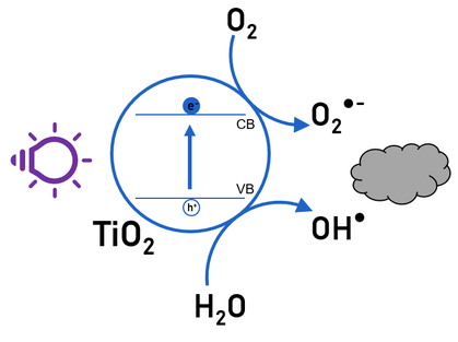
Air/water purification, self-cleaning windows and anti-condensation mirrors all rely on the same principle: photocatalysis. This is the phenomenon where energy of incident UV or visible light is absorbed by a photocatalyst (e.g. TiO2), creating electron-hole pairs. These electrons and holes can interact with adsorbed molecules of the surrounding air resulting in free radicals, which can then react with pollutants and decompose them into smaller, unharmful compounds. In LumiLab, the photocatalytic activity of novel materials is analyzed using a photocatalysis reactor, driven by high power UV LEDs, This photocatalytic treatment is combined with a pre-treatment using a non-thermal atmospheric plasma. We focus on the decomposition of volatile organic compounds, or VOCs, which are present in both indoor air and are emitted in many industrial processes. These VOCs can cause both acute and chronic health effects when present in too high concentrations.
Electronic structure of luminescent materials
Quantum Mechanical Calculations
The functional behavior of luminescent materials is determined by the underlying electronic structure. Studying the latter is hence essential to understand the former. During luminescence processes, electronic excitations accompany the absorption or emission of photons, implying that also the atomic and electronic structures of excited states are of interest.
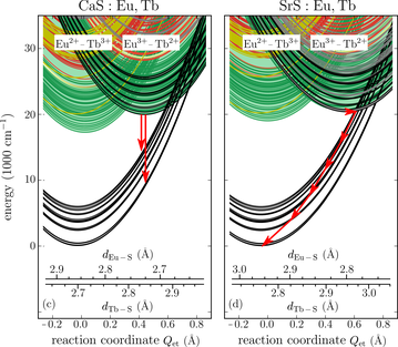
At LumiLab, various electronic structure calculation methods are employed to support experiments, ranging from empirical crystal field models to quantum mechanical methods. The excited states of lanthanide and transition metal impurities in crystals are obtained from first principles using multi-configurational expansions of the many-electron wavefunctions, accounting the strong electron correlations that are archetypal for these elements. Effects of the crystalline environment and special relativistic effects are accounted for via proper embedding potentials and the Douglas-Kroll-Hess two-component Hamiltonian, resulting into accurate electronic spectra and in-depth information on various radiative and non-radiative relaxation channels.
X-ray Absorption Spectroscopy
Electronic structures are also studied experimentally via various X-ray spectroscopy techniques. To this means, campaigns to different beamlines of the European Synchrotron Radiation Facility (ESRF) are regularly organized. The local symmetry, coordination and electronic structure of active centers in luminescent materials are obtained from extended X-ray absorption fine structure (EXAFS) and X-ray absorption near edge structure (XANES) spectroscopy. In addition, X-ray emission (XES) and resonant inelastic X-ray scattering (RIXS) spectroscopy give access to the low-energy excitations that are involved in luminescence processes, including intra- and interconfigurational d-d, f-f and f-d transitions, as well as various kinds of charge-transfer transitions.
Microscopic cathodoluminescence spectroscopy
Since phosphors show a strong correlation between their composition and their optical properties, it is of great interest to look beyond the averaged characteristics resulting from the standard research methods performed on bulk phosphor quantities.
A perfect means for studying phosphors on the microscale is provided by SEM-EDX-CL, where cathodoluminescence (CL) and characteristic X-rays (EDX) are collected simultaneously for nanometer-sized areas scanned by an electron microscope. Correlating this structural, compositional and luminescent information allows for identification of non-uniform doping or impurity phases, which is much-needed input for the improvement of synthesis methods and the overall performance of the phosphor. With the added possibility of temperature- and time-resolved CL spectroscopy this makes for a very powerful tool for characterizing and understanding luminescent materials.

![X-ray absorption spectroscopy on rotating sample Schematic representation of the experimental setup (a): monochromatic x rays strike the rotating sample, the x-ray fluorescence is analyzed by a spectrometer in Rowland geometry, using an array of spherically bent crystal analyzers and an avalanche photodiode. The sample is irradiated by violet or IR lasers and the radioluminescence (RL) is recorded. The schematic representation in (b) illustrates how light of different wavelengths, temperature, and x rays induce electron transfer and hence affect the Eu2+-Eu3+ (blue-red) and Dy2+-Dy3+ (green-yellow) equilibria in the phosphor. (c) Camera image of the rotating sample under steady-state conditions. The x-ray beam hits the sample at point 1. Normalized radioluminescence spectra are displayed (d), measured on three different spots on the rotating sample [indicated in (c)], featuring Eu2+ 4f65d1→4f7 broadband (400–570 nm) and Dy3+ 4f9→4f9 line emissions at around 480, 575, 675, and 760 nm, following the 4F9/2→6HJ (2J=15, 13, 11, 9) transitions, respectively. From Joos J.J., Korthout K., Amidani L., et al. Identification of Dy3+/Dy2+ as electron trap in persistent phosphors. Phys. Rev. Lett. 125, 033001 (2020).](https://www.ugent.be/we/img/WE04/lumilab/img_research.htm/researchesrf.png/@@images/21c2a0c1-d397-4c4f-a02c-b6fbf3ae8b63.png)
![Microscopic cathodoluminescence spectroscopy Scanning electron microscope (SEM) study on a CaS:Eu0.01Tb0.01 powder. Backscattered electron image (a), along with energy-dispersive X-ray (EDX) maps for terbium and europium (b). The colors encode the local terbium (green) and europium (red) concentrations. Simultaneous detection leads to a yellow color. c Cathodoluminescence (CL) spectra for a few selected points that are indicated in d. d False color image, displaying the total integrated CL intensity. e shows how the relative contributions of the red Eu2+ (integrated from 600 to 650 m) and IR (integrated from 760 to 815 m) luminescence band to the total CL spectrum evolve as a function of the local Eu and Tb concentrations, [Eu] ⋅ [Tb]. From Joos, J.J., Van der Heggen, D., Martin, L.I.D.J. et al. Broadband infrared LEDs based on europium-to-terbium charge transfer luminescence. Nat Commun 11, 3647 (2020).](https://www.ugent.be/we/img/WE04/lumilab/img_research.htm/researchcl.png/@@images/eae08dd7-e0fe-43f7-97d9-045de5fad496.png)